

Sub-1 nanometer chip technology has entered a new era after IBM unveiled its latest semiconductor breakthrough. For decades, researchers viewed the one-nanometer threshold as a practical limit. Shrinking transistors further created severe engineering challenges.
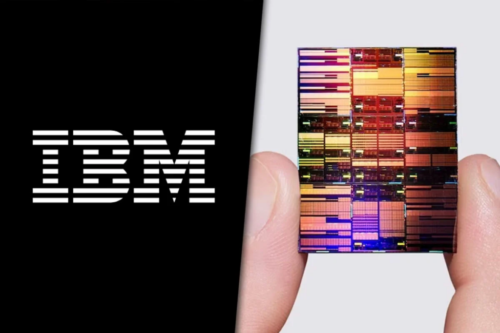
However, IBM now claims it has developed the world’s first sub-1 nanometer chip technology. The company says the prototype packs roughly 100 billion transistors into a fingernail-sized design.
As a result, the achievement could shape faster, more efficient AI hardware during the coming years.
Why the 1-Nanometer Barrier Was Considered Nearly Impossible
For years, chipmakers improved processor performance by shrinking transistors. Smaller components completed more calculations while using less electricity.
Eventually, engineers encountered difficult physical obstacles. Heat became harder to control as transistor density increased. Electrical leakage also reduced efficiency.
Meanwhile, quantum effects complicated reliable operation at extremely small dimensions. Consequently, many researchers believed conventional transistor scaling had reached a practical limit.
Instead, semiconductor companies explored advanced packaging, new materials, and three-dimensional chip designs. Even so, crossing the one-nanometer barrier remained one of the industry’s toughest engineering goals.
How IBM’s Sub-1 Nanometer Chip Reached 100 Billion Transistors
IBM pursued a different strategy. Rather than relying only on traditional scaling, researchers developed a new architecture called NanoStack.
The design stacks transistor components vertically instead of spreading them across a flat surface. Vertical stacking allows engineers to place more transistors into the same area. It also improves communication between nearby components.
As a result, IBM achieved nearly 100 billion transistors on a chip roughly the size of a fingernail. Researchers also combined advanced fabrication techniques with new materials.
According to IBM, the prototype delivers up to 50% higher performance. Alternatively, it can reduce power consumption by up to 70% compared with IBM’s 2-nanometer-class technology under similar conditions.
Why the Sub-1 Nanometer Chip Could Redefine AI Hardware
Artificial intelligence requires enormous computing power. Training advanced AI models demands billions of calculations and substantial electricity. Therefore, efficiency now matters as much as processing speed.
In addition, IBM believes higher transistor density could help future AI accelerators handle larger workloads efficiently. Faster memory access could also reduce performance bottlenecks. Improved SRAM scaling may further support demanding AI tasks.
Moreover, cloud providers could lower operating costs through better processor efficiency. Developers may also build more capable AI systems inside smaller devices. As a result, future data centers could deliver greater computing power while consuming less energy.
What Still Stands Between the Prototype and Commercial Production
Despite the milestone, commercial products will not arrive immediately. Laboratory demonstrations differ significantly from mass production. Manufacturers must develop reliable production methods and improve manufacturing yields.
Also, existing fabrication processes require further refinement. IBM expects industry partners to build future commercial technologies upon the research. Therefore, widespread adoption will likely take several years.
What IBM’s Breakthrough Means for the Future of Computing
IBM’s announcement marks an important milestone for semiconductor research. Commercial deployment still requires additional engineering progress. Nevertheless, the achievement proves engineers can advance beyond limits once considered unreachable.
Furthermore, stronger AI hardware could accelerate innovation across cloud computing, robotics, scientific research, and advanced data analysis. The breakthrough may also inspire further semiconductor discoveries across the industry.
Ultimately, IBM’s sub-1 nanometer chip could help define the next generation of artificial intelligence and high-performance computing while extending future chip innovation.